The continuous evolution of electronic technology has made it possible to develop increasingly compact, powerful, and intelligent devices. From smartphones and wearable electronics to autonomous vehicles and industrial automation systems, modern products depend on electronic circuits that operate accurately and reliably. A key element behind these innovations is the printed circuit board (PCB), which provides the physical structure and electrical pathways needed to connect electronic components.
PCBs help organize complex circuits into compact assemblies while supporting consistent manufacturing and reliable operation. Their design, materials, and layer configurations vary according to the requirements of each application. Understanding what is PCB in electronics provides a foundation for exploring electronic product design, circuit integration, and manufacturing processes.

What is a Printed Circuit Board?
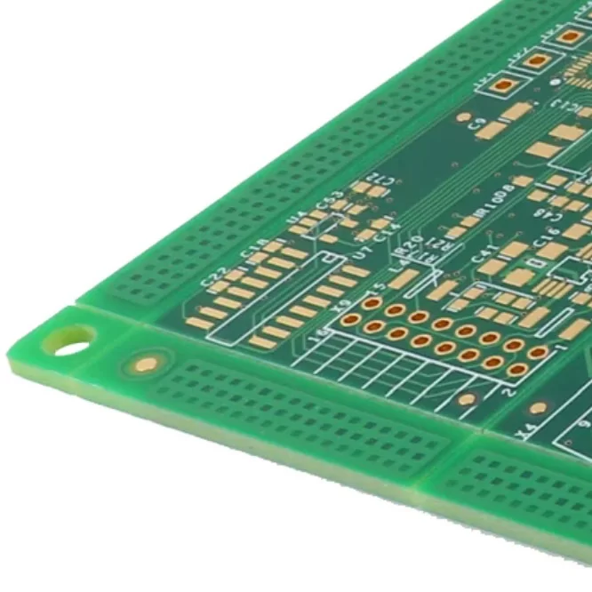
A printed circuit board, commonly abbreviated as PCB, is a board that supports electronic components and connects them through patterned conductive pathways. These pathways, usually made from copper, carry electrical power and signals between components such as resistors, capacitors, integrated circuits, and connectors.
The board combines conductive materials with an insulating substrate to create an organized and mechanically stable circuit structure. Depending on the design, it may contain a single copper layer or multiple conductive layers separated by dielectric materials. Components are attached using soldering or other assembly methods, forming an integrated electronic system.
PCB technology has developed significantly from early circuit-support structures into highly engineered platforms used in nearly every electronic industry. Today, demand for advanced PCBs continues to grow alongside automotive electronics, the Internet of Things (IoT), artificial intelligence (AI), telecommunications, and medical technology. These applications require circuit boards with different levels of complexity, reliability, thermal performance, and signal integrity.
Understanding what is PCB in electronics is therefore essential for engineers, product developers, and manufacturers who need to select suitable board structures and ensure that electronic designs can be produced efficiently.
What are the Different Types of PCBs?
PCBs can be classified according to their conductive layer count, substrate construction, flexibility, and intended application. Choosing the right type affects circuit routing options, board dimensions, mechanical durability, and manufacturing cost. Two common classification methods are based on the number of layers and the type of substrate.
Based on the Number of Layers
The number of copper layers determines how electrical connections are distributed across a PCB. As electronic products become more compact and circuit designs more sophisticated, manufacturers use different layer configurations to meet routing and performance requirements.
1. Single-sided PCB. A single-sided PCB contains a conductive copper pattern on only one side of the insulating substrate. Its relatively simple structure makes it economical to manufacture and suitable for straightforward circuits with limited routing requirements. Typical applications include basic lighting products, calculators, simple control circuits, and certain power supply devices.
2. Double-sided PCB. A double-sided PCB features copper circuitry on both sides of the board. Plated through-holes and other appropriate interconnections allow electrical signals to pass between the conductive layers, giving designers more routing flexibility. This configuration is commonly used in industrial controls, consumer electronics, power electronics, and communication equipment that require greater circuit density than a single-sided design can provide.
3. Multi-layered PCB. A multilayer PCB consists of three or more conductive layers laminated together with insulating materials. Its internal layers can be used for signal routing, ground references, and power distribution, helping designers accommodate complex circuits within a limited footprint. Although multilayer construction generally involves more processing steps and higher manufacturing costs, it is essential for many servers, networking devices, medical instruments, and advanced automotive systems.
Based on Substrate Type
The substrate determines much of a PCB's mechanical behavior, including whether the board retains its shape or can bend to fit a particular installation. Rigid, flexible, and rigid-flex PCBs each provide different advantages.
1. Rigid PCB. A rigid PCB uses a solid substrate, commonly FR-4, that maintains a fixed shape during handling and operation. Its stable structure supports component mounting and is suitable for a broad range of electronic products, including computers, household appliances, automotive control units, and industrial equipment. Rigid boards are widely used because they offer a practical balance of mechanical strength, manufacturing availability, and cost.
2. Flex PCB. A flexible PCB is manufactured using bendable materials such as polyimide, together with appropriately designed copper conductors. It can follow curved surfaces or fit into narrow spaces where a conventional rigid board would be difficult to install. Flexible circuits are common in wearable devices, cameras, display connections, medical electronics, and compact products that benefit from reduced wiring and connector requirements.
3. Rigid-Flex PCB. A rigid-flex PCB integrates rigid circuit sections with flexible interconnections in one assembly. This design supports compact three-dimensional packaging and can reduce the need for separate cables or connectors between circuit sections. Rigid-flex boards are particularly useful in aerospace systems, medical equipment, specialized industrial electronics, and other applications where space constraints and connection reliability are important.

What are the Different PCB Layers?
A PCB may contain several functional layers, each designed to support electrical connectivity, insulation, protection, or assembly. The exact stack-up depends on whether the board is single-sided, double-sided, or multilayer. Understanding these layers helps explain how a PCB achieves its electrical and mechanical properties.
1. Dielectric Layer. The dielectric layer is the electrically insulating material that separates conductive copper layers. FR-4, a glass-fiber-reinforced epoxy laminate, is widely used because it provides useful mechanical strength, electrical insulation, and thermal performance. Other materials may be selected when an application requires flexibility, high-frequency characteristics, or improved thermal behavior.
Within multilayer PCB construction, dielectric materials commonly include the following:
Core. A core is a cured laminate consisting of an insulating substrate with copper foil bonded to one or both sides. It provides structural support and forms part of the board's electrical stack-up. Depending on the design, multiple cores may be combined to create a multilayer structure.
Prepreg. Prepreg is a glass-fiber material impregnated with partially cured resin. During lamination, heat and pressure soften and cure the resin, bonding the PCB layers together while maintaining electrical insulation between conductive sections. Its thickness and resin characteristics influence the final stack-up and manufacturing results.
2. Copper Layer. Copper layers form the conductive circuitry of a PCB. They contain traces, pads, and, where applicable, copper planes used for signal transmission, power distribution, and grounding. In multilayer designs, internal copper layers can help manage routing density and provide reference planes for improved signal integrity. Copper thickness and trace geometry must be selected according to electrical current, thermal requirements, and manufacturing tolerances.
3. Solder Mask. The solder mask is a protective coating applied over selected areas of the outer copper layers. It helps reduce oxidation and contamination while insulating nearby conductors to lower the risk of accidental solder bridges. Openings are created over pads and other locations that must remain exposed for component assembly or electrical contact. Although green is a common solder mask color, other colors are available depending on the manufacturing requirements.
4. Surface Finish. The surface finish protects exposed copper pads and helps maintain solderability before and during PCB assembly. Common options include Hot Air Solder Leveling (HASL), Electroless Nickel Immersion Gold (ENIG), immersion tin, and Organic Solderability Preservative (OSP). Each finish offers different characteristics related to cost, surface flatness, storage life, and compatibility with component packages. The selection should reflect the assembly process and the intended operating environment.
How are PCBs Fabricated?
PCB fabrication converts circuit design data and raw materials into a finished bare board that is ready for component assembly. The precise workflow depends on the board's layer count and technical specifications. The following stages describe the principal steps involved in producing a basic PCB, with additional operations required for more complex multilayer designs.
PCB Schematics and Layout Generation. The process begins with a schematic that defines the circuit components and their electrical relationships. Engineers then create the PCB layout using electronic design automation software, determining component positions, copper routing, pad geometry, and board dimensions. Design rule checks and manufacturing reviews help identify spacing violations, unsuitable hole sizes, and other potential problems before production begins.
Panel Preparation. The selected substrate is prepared in a suitable panel format for fabrication. Manufacturers often arrange multiple board designs or repeated units on a larger production panel to improve material utilization and processing efficiency. Panelization details, including tooling holes, fiducials, and separation methods such as V-scoring or tab routing, are planned according to the board design and assembly requirements.
Etching. The copper pattern is formed by selectively removing unwanted copper from the laminate. A protective resist defines the areas that must remain conductive, while an etching solution removes the exposed copper. After the resist is removed, the remaining copper forms the intended circuit traces and pads. For multilayer boards, inner-layer imaging and etching generally take place before lamination, while outer-layer circuits are patterned at a later stage.
Board Drilling. Holes are produced to accommodate through-hole component leads, mounting hardware, and electrical connections between layers. Computer-controlled drilling equipment follows the specified drill data to achieve the required hole locations and dimensions. Mechanical drilling is widely used for standard holes, while laser drilling can create small microvias for high-density interconnect applications. Hole quality and positional accuracy are important for reliable assembly and interlayer connectivity.
Electroplating. For boards that require plated through-holes or other plated features, a conductive copper layer is deposited onto prepared hole walls and designated surfaces. This creates electrical connections between the relevant conductive layers. Plating conditions must be controlled to achieve suitable copper thickness and coverage, as incomplete plating or voids can compromise electrical reliability.
Solder Masking. After the copper circuitry has been formed and the required processing steps completed, a solder mask is applied to protect the board surface. The coating is patterned to leave component pads and other designated contact areas exposed. Depending on the selected material, the process may include coating, pre-drying, imaging, development, and final curing. Surface finishing is a separate operation that is subsequently applied to exposed copper pads.
Testing. Bare PCBs undergo inspection and electrical testing before being released for assembly. Automated optical inspection (AOI) can identify visible pattern defects, while electrical tests check for unintended shorts and open connections. Flying probe testing uses movable probes to contact designated test points and is useful for many prototype and low-volume applications. Fixture-based testing, including bed-of-nails systems, may be selected for higher-volume production. The test method depends on the board design, production volume, and quality requirements.
Conclusion
Understanding what is PCB in electronics helps explain how electronic components are interconnected and why board construction plays such an important role in product performance. Different PCB types serve different design requirements, while the dielectric, copper, solder mask, and surface finish each contribute to the board's function and reliability. From schematic development to etching, drilling, plating, and electrical testing, every fabrication stage must be carefully controlled to achieve consistent results.