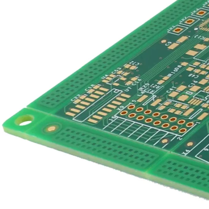
Printed circuit boards are essential to modern electronic systems, providing the physical platform that connects and supports electronic components. From simple consumer devices to sophisticated industrial equipment, a well-designed PCB helps ensure stable electrical performance, efficient use of space, and reliable operation. The quality of the design also influences manufacturing complexity, assembly efficiency, and the overall cost of the finished product.
For beginners, understanding how to design a PCB may initially seem challenging because the process involves electrical engineering, component selection, layout planning, and manufacturing considerations. However, dividing the work into manageable stages makes the process easier to understand and follow. This guide walks through the main steps of PCB design, from defining project requirements to validating a prototype, helping you develop a design that meets functional needs and can be manufactured efficiently.

What is PCB Design?
PCB design is the engineering process of converting an electronic circuit concept into a physical board layout that can be fabricated and assembled. It involves defining electrical connections, selecting suitable components, arranging their positions, routing copper traces, and preparing the files required for production.
The complexity of the work depends on the application. A basic single-layer board may require relatively straightforward routing, while a multilayer PCB used in high-speed or high-density electronics needs careful planning for signal integrity, power distribution, thermal performance, and electromagnetic compatibility. Learning how to design a PCB therefore requires both an understanding of circuit fundamentals and familiarity with electronic design automation (EDA) software. A structured design approach helps reduce errors, improve manufacturability, and produce reliable electronic hardware.
How is a PCB Designed?
A successful PCB design process follows a series of connected stages. Each stage builds on the decisions made earlier, so requirements, circuit logic, component placement, and manufacturing constraints should be considered together rather than treated as separate tasks.
1. Defining the Purpose and Requirements
Begin by identifying what the PCB needs to do and the conditions under which it will operate. Define its main functions, required interfaces, power supply characteristics, expected current levels, physical dimensions, and installation constraints. Environmental factors such as temperature, humidity, vibration, and potential electromagnetic interference should also be considered when relevant.
The project requirements should identify applicable safety or industry standards, reliability expectations, and any cost or production-volume limits. These details help guide component selection, material choices, and board configuration. A clear specification at the beginning makes later design decisions more consistent and reduces the likelihood of expensive revisions.
2. Schematic Circuit Diagram
Once the functional requirements are established, create a schematic that represents the electrical relationships between components. The schematic defines how devices such as integrated circuits, resistors, capacitors, connectors, and power components interact within the circuit. EDA platforms such as Altium Designer, Autodesk EAGLE, and other suitable tools help designers build and validate this representation before moving to the physical layout.
When preparing the schematic, pay attention to the following tasks:
Place the required components: Select appropriate parts based on electrical ratings, functionality, availability, and project requirements.
Establish electrical connections: Connect the components according to the circuit design and ensure that signal paths and power connections are represented correctly.
Define grounding and power networks: Assign suitable power and ground connections while considering current requirements, noise sensitivity, and voltage levels.
Add clear labels and annotations: Use meaningful component references, net names, and notes to make the schematic easier to review and maintain.
Run an Electrical Rules Check (ERC): Check for common schematic issues, such as unconnected pins, conflicting connections, or incorrectly defined electrical properties.
A complete and well-organized schematic provides the foundation for an accurate PCB layout and makes design verification more efficient.
3. Design PCB Layout
After the schematic is ready, the next task is to transform the electrical connections into a physical board. PCB layout design determines where components are placed, how copper traces connect them, and how the board's layers are organized. Software such as KiCad, Altium Designer, and OrCAD provides tools for arranging components, routing signals, and checking layout constraints.
A reliable layout should satisfy electrical and mechanical requirements while accounting for heat dissipation, signal quality, assembly access, and manufacturing capabilities. The following activities are central to this stage.
Determine the Board Configuration
Establish the board outline, dimensions, mounting locations, and number of copper layers needed for the circuit. A single-layer or double-layer PCB may be suitable for simpler applications, while multilayer construction can support denser routing and more controlled electrical performance. Select the substrate according to operating frequency, thermal requirements, mechanical strength, and budget. FR-4 is widely used for general-purpose electronics, while PTFE-based materials may be appropriate for certain high-frequency applications.
Component Arrangement
Place components according to their electrical relationships, functional groups, and physical constraints. For example, power conversion circuits, sensitive analog sections, and high-frequency components may require careful separation or specific placement strategies. Keep critical connections practical, provide suitable space around components, and consider access for soldering, inspection, and rework. Heat-generating devices should be positioned with appropriate thermal management in mind.
Tracking and Routing
Route copper traces to connect components while meeting current-carrying, clearance, and signal-integrity requirements. Trace width should reflect the expected current and acceptable temperature rise, while spacing must comply with the design rules and relevant electrical requirements. Minimize unnecessary routing detours, avoid abrupt geometry where it could affect sensitive signals, and prioritize critical nets such as high-speed signals, clocks, and power connections. Routing should also account for return-current paths and potential crosstalk between neighboring traces.
Grounding Level
A carefully planned ground structure provides return paths for circuit currents and helps manage noise. Depending on the board architecture, designers may use ground planes, ground regions, or dedicated ground connections. A continuous reference plane is often beneficial for high-speed signals because it can reduce return-path discontinuities and help control electromagnetic emissions. Grounding decisions should be coordinated with power distribution, analog and digital circuit requirements, and the overall layer stack.
Stack up Design
The layer stack-up defines the order, thickness, and materials of the copper and insulating layers in a multilayer PCB. It determines how signal layers relate to ground and power planes and influences impedance control, crosstalk, electromagnetic interference, and thermal behavior. A suitable stack-up should be planned early, particularly for high-speed, high-frequency, or impedance-controlled designs. The final configuration must also align with the PCB manufacturer's available materials, fabrication tolerances, and production capabilities.

4. Design Verification
Before releasing a PCB design for production, verify that it satisfies the electrical, mechanical, thermal, and manufacturing requirements. EDA tools can run Design Rule Checks (DRC) to identify layout violations, while simulation and engineering analysis may help assess signal behavior, power integrity, or thermal performance where necessary.
Design for Manufacturability (DFM) review is another important part of this stage. It evaluates whether the layout can be produced and assembled reliably using the selected manufacturing processes. Common verification tasks include:
Verify electrical, thermal, and mechanical performance: Review power distribution, critical signal paths, heat dissipation, mounting points, and enclosure compatibility.
Check minimum track width and spacing: Confirm that copper features meet the capabilities of the intended fabrication process.
Check hole sizes and pad dimensions: Verify drill diameters, annular rings, pad sizes, and other relevant manufacturing constraints.
Review electrical clearances: Ensure that the spacing between conductive features meets the design requirements and reduces the risk of unintended shorts.
Ensure proper layer alignment and stack-up: Confirm that the layer structure, via connections, and registration requirements are suitable for fabrication.
Review component placement and assembly access: Check component spacing, orientation, polarity, and accessibility to reduce assembly and inspection difficulties.
Check silkscreen information: Make sure reference designators, polarity marks, and other printed labels are legible and do not interfere with pads or exposed conductive areas.
Passing automated checks is important, but it does not guarantee that every design issue has been resolved. A final engineering review and, where appropriate, a manufacturer-led DFM assessment can identify additional risks before production begins.
5. Preparing Manufacturing Files (Gerber Files)
Once the layout has been verified, prepare the documentation and output files needed for PCB fabrication and assembly. Gerber files are commonly used to communicate the board's individual manufacturing layers, including copper patterns, solder mask, and silkscreen. Drill data is typically provided in a compatible numerical control format, while board outline information and fabrication notes communicate important mechanical requirements.
PCB assembly requires additional documentation, which may include a bill of materials (BOM), component placement or pick-and-place files, and assembly drawings. These files serve different purposes: Gerber and drill files support bare-board fabrication, whereas BOM and placement data support component sourcing and assembly.
Before sending the files to a manufacturer, verify that the output settings, units, layer names, board dimensions, and drill information are consistent. It is also helpful to provide stack-up details, impedance requirements, material specifications, surface finish preferences, and other production notes when applicable. Coordinating with the manufacturer at this stage helps identify capability mismatches early and reduces the risk of delays caused by incomplete or incorrect documentation.
6. Prototype
Building a prototype allows the design to be evaluated under practical conditions before moving to larger production quantities. Prototype testing can reveal issues that may not be apparent in the schematic or layout, including incorrect connections, unexpected electrical behavior, component interference, thermal problems, and assembly difficulties.
Testing should follow the project's requirements and may include power-up checks, functional testing, interface validation, signal measurements, and mechanical fit assessments. If the board does not meet expectations, investigate the cause and update the schematic, layout, or component selection as needed. The revised design should then be checked again before release.
Prototype validation is a valuable part of learning how to design a PCB because it connects theoretical design decisions with real-world performance. Finding and correcting problems early can reduce the cost and disruption associated with later manufacturing changes.
Conclusion
Designing a PCB involves more than connecting electronic components. It requires a systematic approach that brings together functional requirements, schematic development, component placement, routing, design verification, and manufacturing preparation. Every stage contributes to the electrical performance, manufacturability, and long-term reliability of the finished board.
By following a structured PCB design process and applying appropriate DRC and DFM checks, designers can identify potential issues before fabrication and improve the chances of achieving a successful result. Prototype testing further helps confirm that the board performs as intended and provides useful feedback for refinement. Combining sound engineering principles with careful validation creates a stronger foundation for reliable, scalable electronic products.