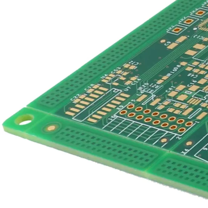
Printed circuit board manufacturing and assembly involve two closely related stages: preparing the bare board and installing the electronic components. Each stage contributes to the functionality and reliability of the finished product. A PCB provides the structural base for electronic components, while its conductive copper patterns establish the electrical pathways that allow these components to work together.
From an engineering perspective, component connections depend on copper traces, pads, vias, and solder joints. Package specifications, component orientation, polarity, and connection requirements must all be considered during design and assembly. Understanding how to connect components on PCB correctly helps reduce assembly defects and supports stable electrical performance. For more information about identifying electronic parts, see this guide on how to identify PCB components on a board.

What are Categories & Mounting Techniques Used in Connecting Components on PCB?
Electronic components are available in different package styles to accommodate various electrical requirements, board dimensions, and assembly methods. Two widely used categories are pin-through-hole (PTH) components and surface-mount devices (SMDs). Each type uses a different mounting approach, so selecting the correct process is an important part of PCB assembly.
PTH components have leads that pass through drilled holes in the circuit board. Their leads are soldered to conductive pads, creating both mechanical attachment and electrical connections. This mounting style is still used for components that require strong mechanical support or have particular electrical or thermal requirements. Depending on the application, PTH parts may be installed manually or processed using suitable automated assembly equipment.
SMD components, by contrast, are mounted directly onto conductive pads on the PCB surface. They generally do not require dedicated lead-insertion holes, allowing components to be positioned more densely. Their compact packages also support automated assembly, making surface-mount technology widely used in modern electronics manufacturing. The appropriate mounting method depends on the component package, circuit design, mechanical requirements, and production process.
The Process of Connecting Components on PCB
The process of connecting electronic components to a PCB begins with circuit planning and continues through component placement, soldering, and final inspection. Each stage must be completed carefully to ensure that the assembled board matches the design and performs as intended.
1. Circuit Design and PCB Layout Preparation
PCB assembly starts with a circuit design based on the product's functional requirements. Engineers identify the required components, define their electrical relationships, and convert the schematic into a physical PCB layout. During this stage, component footprints, pad dimensions, pin assignments, polarity markings, and placement orientation must match the selected parts and their datasheets.
For PTH components, the layout specifies the drill locations and finished hole dimensions needed to accommodate the component leads. The pads and surrounding copper must follow the design's electrical and manufacturing rules to prevent unintended connections. For SMD components, accurately sized pads and suitable spacing provide the surfaces needed for placement and soldering.
The layout should also account for trace widths, electrical clearances, thermal management, and assembly access. Checking these details before manufacturing helps prevent shorts, incorrect connections, and component-mounting problems. A complete and accurate design provides a reliable foundation for understanding how to connect components on PCB throughout the assembly process.
2. Components Placement on PCB
Component placement depends on the package type, the board design, and the selected assembly method. Proper positioning ensures that each component aligns with its designated pads or holes and maintains the required electrical and mechanical relationships.
PTH components are commonly inserted through their corresponding holes. Before insertion, their leads may need to be trimmed or formed according to the assembly instructions and component specifications. During placement, technicians must verify the component's reference designation, polarity, orientation, and lead alignment. The component should be seated as intended by the design rather than positioned at an arbitrary height, since mounting height can affect mechanical stability and assembly quality.
SMD components are generally placed using automated pick-and-place equipment in production environments. First, solder paste is deposited onto the designated pads through a stencil-printing process. A programmed machine then picks components from feeders and positions them on the paste-covered pads according to the placement data. Accurate alignment is essential, particularly for small packages and fine-pitch devices.
After placement, the board usually enters a reflow oven, where the solder paste is heated according to a controlled temperature profile to form solder joints. This process supports consistent results across large production runs. Depending on the assembly design, PTH components may be inserted and soldered in a subsequent operation, although the exact sequence varies with the board and manufacturing requirements.
3. Soldering Process
Soldering establishes the electrical and mechanical connections between PCB pads and component leads or terminals. The chosen technique depends on the package type, component sensitivity, board design, and production volume. Common methods include reflow soldering for SMD components, wave soldering for suitable through-hole assemblies, and selective or manual soldering for specific applications.
For reflow soldering, solder paste is applied to the pads before components are placed. The board then passes through a controlled heating cycle that melts the solder and allows it to form joints as the assembly cools. Correct temperature control and conveyor settings help reduce defects such as insufficient wetting, solder bridging, and component displacement.
Wave soldering is often used for compatible PTH assemblies. The PCB travels through a machine that brings its solderable surfaces into contact with a controlled wave of molten solder. The solder wets the prepared joints and solidifies as the board moves through the process. Depending on the product, selective soldering or manual soldering may be used when only particular areas require through-hole connections or when automated wave soldering is unsuitable.
Regardless of the technique, solder joints should be formed according to the applicable process specifications. Proper control of soldering temperature, flux application, board handling, and cooling helps produce reliable connections and reduces the likelihood of assembly defects.
4. Testing & Validation of the Connections
Inspection and testing should be incorporated throughout PCB manufacturing and assembly rather than postponed until the end. Early checks can identify design, material, and placement problems before they affect a completed board. During incoming inspection, manufacturers can verify that the bare PCB and electronic components meet the relevant specifications.
Before assembly, the board should be checked for visible damage, incorrect dimensions, defective holes, and broken or incomplete conductive features. During component placement, inspection should confirm that parts are correctly oriented, aligned, and positioned. After soldering, joints should be examined for issues such as insufficient solder, bridging, poor wetting, or other defects appropriate to the package and soldering process.
Once assembly is complete, electrical tests can verify continuity and identify unintended shorts or open circuits. Functional testing then checks whether the assembled PCB operates according to its intended requirements. Depending on the product, manufacturers may also use automated optical inspection (AOI), X-ray inspection, in-circuit testing, or other methods suited to the assembly. Combining appropriate inspection techniques helps improve quality and supports reliable PCB performance.

Key Points to Recall
Maintain accurate component information: Ensure that the schematic, PCB layout, bill of materials, and assembly data use consistent part numbers, footprints, and reference designators.
Follow proper handling and storage procedures: Protect sensitive components from electrostatic discharge and follow the moisture-control requirements specified for moisture-sensitive devices.
Use flux and cleaning materials appropriately: Select compatible flux products and remove residues when required by the flux specification, assembly process, or product cleanliness requirements.
Remove excess flux and contaminants when necessary: Use a compatible cleaning method, such as an approved IPA-based process, where appropriate. Follow the cleaner manufacturer's safety instructions and allow the board to dry fully.
Plan for thermal management: Identify heat-generating components and provide suitable copper areas, thermal vias, heatsinks, or other cooling measures where the design requires them.
Inspect solder joints carefully: Check for visible soldering defects and use additional inspection methods when component packages or reliability requirements call for them.
Verify circuit functionality: Perform suitable electrical and functional tests to confirm that the components are connected correctly and the assembled PCB meets its specifications.
Summary
Connecting electronic components to a circuit board is a fundamental part of PCB assembly. Every component must be installed in the correct position and connected to the intended conductive features to achieve the required electrical behavior. From circuit design and PCB layout preparation to component placement, soldering, and final testing, each stage contributes to the quality and reliability of the completed assembly.
A consistent assembly process combines accurate design data, suitable mounting techniques, controlled soldering conditions, and systematic inspection. As electronic components continue to evolve toward smaller packages and more complex functionality, manufacturers must also adapt their placement equipment, soldering processes, and quality-control methods. By following appropriate engineering and manufacturing practices, designers and assemblers can reduce defects and produce dependable PCBs for a wide range of applications.