
6L HDI Portable Electron PCB


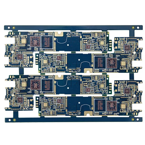
Advanced 6-Layer HDI Portable Electronics PCB Manufacturing & High-Density Interconnect Solutions
Engineered specifically for next-generation handheld devices, compact smart equipment, and high-performance portable consumer electronics, PrintedBoardAssembly delivers precision-crafted 6L HDI Portable Electron PCBs. By utilizing advanced 1+N+1 High-Density Interconnect (HDI) architecture, micro-via laser drilling, and premium FR-4 ITEQ IT180A material, our multi-layer circuit boards maximize routing density and electrical performance within extremely restricted physical footprints.
Comprehensive Technical Specifications & Material Parameters
To support ultra-fine pitch components, high-speed data transmission, and rigorous spatial limitations in portable hardware, our 6-layer HDI circuit boards are fabricated under strict industrial standards and stringent quality controls:
Product Model & Structure: 6L (1+N+1) High-Density Interconnect (HDI) PCB
Substrate Material: High-Tg FR-4 ITEQ IT180A laminate (offering exceptional thermal stability, CAF resistance, and superior reliability during multiple reflow cycles)
Layer Configuration: 6 Layers featuring a 1+N+1 build-up (enabling blind and buried via connections for advanced space-saving routing)
Solder Mask & Legend Color: Green solder mask with high-contrast White silkscreen labeling
Finished Board Thickness: Ultra-slim 0.8mm profile (optimized for lightweight, low-profile portable device enclosures)
Finished Copper Thickness: Inner layers 1OZ / Outer layers 0.5OZ (balanced for optimal signal integrity and efficient power distribution)
Surface Treatment: Electroless Nickel Immersion Gold (ENIG 1-2u") providing a flat coplanar surface, excellent wire-bonding capability, and superior oxidation resistance
Min Trace / Space: 3mil / 3mil precision etching for high-density breakout routing
Min Hole Dimension: Mechanical hole size 0.2mm alongside laser micro-vias
Primary Application: Portable electronic devices, smart handheld terminals, and compact wireless hardware
Engineering Architecture & Core Advantages of 6L 1+N+1 HDI PCBs
Traditional multi-layer through-hole PCBs often fail to meet the miniaturization and signal speed requirements of modern portable electronics. The implementation of 1+N+1 HDI architecture transcends these limitations through advanced micro-via technology:
Ultra-Compact Spatial Efficiency: Utilizing laser-drilled blind and buried vias allows component pins to be placed closer together, drastically reducing overall board dimensions and weight.
Enhanced Signal Integrity at High Frequencies: Shorter interconnection paths minimize parasitic capacitance and inductance, ensuring clean, low-loss signal propagation for high-speed processors and communication modules.
Superior Thermal & Mechanical Reliability: Fabricated with high-Tg ITEQ IT180A material, these boards withstand aggressive thermal stresses without delamination, ensuring long-term durability in handheld environments.
Optimized Routing Density: The 1+N+1 build-up provides dedicated routing channels on outer and inner layers, eliminating routing congestion even when interfacing with complex BGA packages.
Flat Surface Planarity: Immersion Gold (ENIG) surface treatment guarantees flat pad interfaces, ensuring flawless solder joint formation during fine-pitch SMT assembly.
Overcoming Manufacturing Challenges: Precision Processing
Manufacturing 6-layer 1+N+1 HDI circuit boards requires highly specialized equipment and strict process parameters compared to standard rigid boards. Laser ablation depth control, sequential lamination cycles, micro-via copper filling, and precise registration alignment are critical to preventing internal voids or open circuits.
At PrintedBoardAssembly, we utilize advanced UV/CO2 laser drilling systems, automated optical alignment fixtures, and vacuum lamination presses to master these complexities. This rigorous process control ensures perfect layer-to-layer registration, complete via barrel plating, and absolute electrical dependability for mission-critical portable electronics.
Rigorous Quality Assurance & Multi-Stage Testing Protocols
Zero-defect manufacturing is essential for consumer electronics and portable equipment deployed in daily commercial use. Every production batch of 6L HDI Portable Electron PCBs undergoes an exhaustive testing regime prior to dispatch:
Automated Optical Inspection (AOI): High-resolution laser scanning of inner and outer layers to detect trace anomalies, etching defects, or bridging before lamination.
X-Ray Inspection: Non-destructive verification of multi-layer alignment and internal micro-via registration.
Flying Probe Electrical Testing: 100% open and short-circuit verification confirming complete electrical continuity across all complex nets.
Thermal Shock & Solderability Testing: Simulating aggressive assembly environments to guarantee robust joint reliability and board integrity.
Extensive Industry Applications
Our 6-layer HDI circuit boards are trusted across a wide spectrum of compact, high-performance technology sectors:
Portable Consumer Electronics: Advanced smartphones, tablets, handheld gaming consoles, and smart wearable gadgets.
Wireless Communication Terminals: Compact RF modules, Bluetooth accessories, and portable satellite tracking devices.
Medical & Diagnostic Tools: Handheld patient monitors, portable ultrasound probes, and diagnostic data loggers.
Industrial Handheld Hardware: Mobile barcode scanners, field-service data terminals, and portable test instrumentation.
Turnkey SMT Assembly & Manufacturing Capabilities
As a premier Electronic Manufacturing Service (EMS) provider, PrintedBoardAssembly offers an integrated, end-to-end manufacturing workflow. Combining precision bare-board fabrication with high-speed Surface Mount Technology (SMT) and Through-Hole (DIP) assembly, we manage everything from component sourcing to final functional testing.
Equipped with advanced pick-and-place machinery, automated solder paste inspection (SPI), multi-zone convection reflow ovens, and real-time AOI verification, we seamlessly execute fine-pitch IC placement, micro-BGA mounting, and compact module integration. Partner with PrintedBoardAssembly to optimize your supply chain, accelerate your time-to-market, and ensure absolute hardware dependability. Contact our engineering team today to review your Gerber files and secure a rapid prototype quotation.


If you have any camping barbeque equipment inquiry, please feel free to contact us.
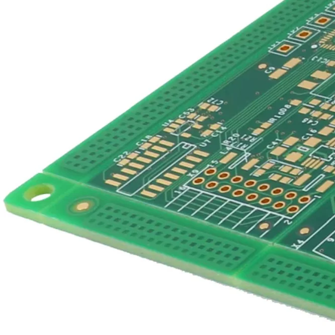
FR-4 stands out as one of the most versatile options. The composition of an FR-4 printed circuit board comprises a woven glass fabric reinforcement impregnated with a flame-retardant epoxy resin binder.

PCB type: Rigid PCB
Layer: Multi-layer
Base material: FR-4
Solder mask: Green
Silk screen: White
Surface treatment: HASL
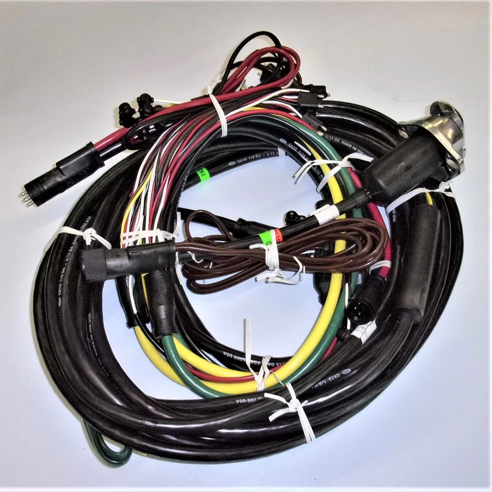
A truck wire harness is like the nervous system of a truck. It is a group of wires, connectors, and terminals that link all the electrical parts together.

Printed circuit board (PCB) defects can interrupt electrical signals, affect system stability, and prevent electronic devices from operating as intended.

Printed circuit boards are essential to modern electronic systems, providing the physical platform that connects and supports electronic components.

Printed circuit board manufacturing and assembly involve two closely related stages: preparing the bare board and installing the electronic components.


